Arduino as ISP
Programming the Standalone ATmega328P
DE6417 Microcontrollers 2 · Week 13
Why Program a Bare Chip?
The Arduino board is a development tool
Everything on the Arduino board around the ATmega328P chip exists to make programming convenient — not to run your final product.
- Real products are built around the chip itself, soldered onto a custom PCB
- Cost: An ATmega328P chip costs ~$2. An Arduino Uno costs ~$25. You ship the chip, not the board.
- Size: The chip is 3 cm long. The Uno board is 7× bigger.
- Power: The Uno's USB-serial chip and regulators draw current even when idle
- Flexibility: On a custom PCB you place only the components your circuit needs
Ways to get code onto a bare ATmega328P
| Approach | Hardware needed |
|---|---|
| Arduino as ISP | Another Arduino Uno running a sketch |
| Dedicated ISP programmer | USBasp, AVRISP mkII, Atmel-ICE |
| Bootloader + USB-serial adapter | FTDI adapter; bootloader must be burned first |
| Bootloader + Uno as carrier | Remove the Uno's chip, seat the target chip in its socket |
| JTAG / debugWIRE | Atmel-ICE; adds hardware debugging |
Today's Approach: Arduino as ISP
Why Arduino as ISP?
- No extra hardware to buy — you already have an Arduino Uno
- Works on macOS, Windows, and Linux without special drivers
- Supported natively by the Arduino IDE and avrdude
- Can both upload sketches and burn bootloaders — the most versatile option with what we have
🛒 Components for Today
| Component | Value / Type | Qty | Part |
|---|---|---|---|
| Arduino Uno | Any revision | 1 | 1 & 2 |
| ATmega328P-PU | DIP-28 package | 1 | 1 & 2 |
| Breadboard | Full or half size | 1 | 1 & 2 |
| Electrolytic capacitor | 10 µF | 1 | 1 |
| Jumper wires | Male-to-male | 6+ | 1 |
| Crystal oscillator | 16 MHz | 1 | 2 |
| Ceramic capacitor | 22 pF | 2 | 2 |
Learning Outcomes
Understand ISP
Explain the ISP protocol and how it differs from the bootloader upload path.
Configure programmer
Flash the ArduinoISP sketch to a Uno and configure the IDE correctly.
Wire correctly
Connect all 6 ISP lines between the programmer Uno and the target chip.
Flash and prove
Upload a sketch to the standalone chip and observe it running independently.
Quick Check — Before We Start
Q1: What does ISP stand for?
Q2: Which physical interface does ISP use?
Two Ways to Program the ATmega328P
ISP writes directly to flash. The chip does not need to be running any code.
What is ISP?
In-System Programming
- A standard AVR hardware feature — not software
- Uses 4 SPI lines to read and write flash, EEPROM, and fuse bits
- Available on every ATmega328P — even a blank, factory-fresh chip
- The programmer holds RESET LOW to put the chip in programming mode, then clocks data in via MOSI
Example: you accidentally set the wrong clock-source fuse — the chip now expects an external crystal that isn't there. Every power-up, the CPU stalls before a single line of code runs, so the bootloader never starts and Serial upload is permanently dead. ISP bypasses all of that: the programmer drives RESET LOW, sends the SPI clock from outside, and reads/writes flash directly. It restores the correct fuse, burns a fresh bootloader, and hands the chip back working — without the chip ever needing to run code first.
The 4 ISP pins on ATmega328P
| Signal | Port / Pin | Physical DIP Pin |
|---|---|---|
| MOSI | PB3 | 17 |
| MISO | PB4 | 18 |
| SCK | PB5 | 19 |
| RESET | PC6 | 1 |
Same pins as SPI — students already know these from earlier in the course.
SPI Recap: Master and Slave Roles
Who is who today
- Master: Programmer Uno (running ArduinoISP sketch)
- Slave: Target ATmega328P on the breadboard
| Target signal | Programmer Uno pin | Direction | Purpose |
|---|---|---|---|
| MOSI | D11 / COPI (Controller Out, Peripheral In) | Master → Slave | Programming data to target |
| MISO | D12 / CIPO (Controller In, Peripheral Out) | Slave → Master | Status and verify data back |
| SCK | D13 / SCK (same name) | Master → Slave | Clock — synchronises every bit |
| RESET (PC6, pin 1) | D10 / SS (repurposed to drive target RESET) | Master → Slave | Hold LOW to enter programming mode |
(ArduinoISP sketch)
(standalone chip)
MISO direction is from the slave's perspective — data comes back from the target to confirm what was written.
Signal Direction Check
Match each signal to its correct direction during ISP programming
The ArduinoISP Sketch
What it does
- A sketch you flash to the programmer Uno — once, before the lab
- Turns that Uno into a protocol translator between your PC and the target chip
- Translates STK500v1 serial commands from avrdude into SPI signals to the target
File → Examples → 11.ArduinoISP → ArduinoISP
ArduinoISP sketch
standalone chip
The 10 µF Capacitor — Critical Detail
Why it's needed
- When avrdude opens the serial port, it pulses the DTR line
- DTR normally travels through the auto-reset circuit and resets the Uno
- A reset mid-programming crashes ArduinoISP → upload fails
- A 10 µF capacitor blocks the brief DTR pulse from reaching RESET
NOT on the target chip.
Wiring the capacitor
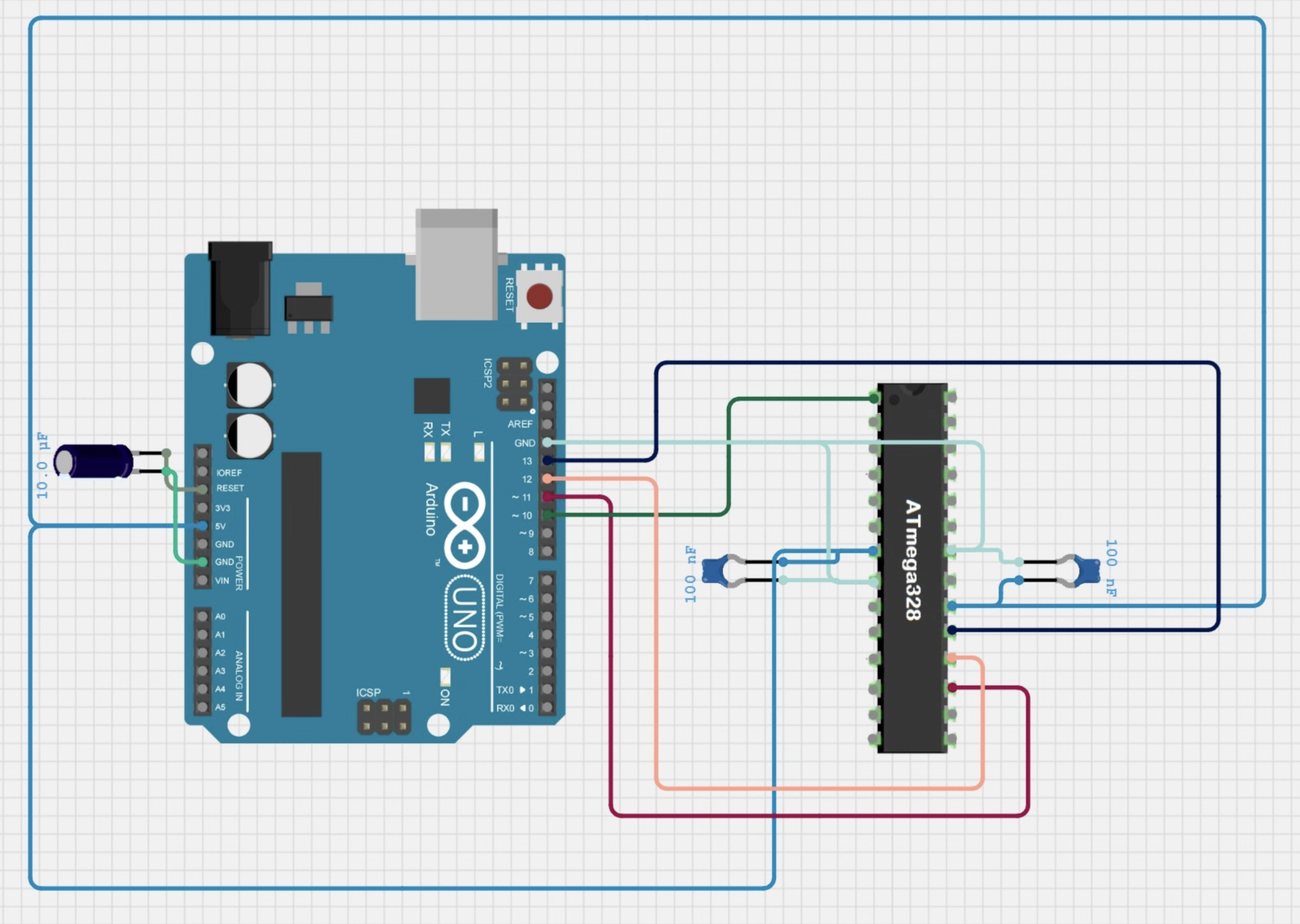
Wiring: Full Connection Table
| Programmer Uno Pin | Signal | Target ATmega328P DIP Pin | Note |
|---|---|---|---|
| Pin 10 | RESET | Pin 1 (PC6) | Pulls target into programming mode |
| Pin 11 | MOSI | Pin 17 (PB3) | Data out from programmer |
| Pin 12 | MISO | Pin 18 (PB4) | Data back from target |
| Pin 13 | SCK | Pin 19 (PB5) | Also the programmer Uno's onboard LED — it flickers during upload (normal) |
| 5V | VCC | Pin 7 + Pin 20 | Power the target from the programmer |
| GND | GND | Pin 8 + Pin 22 | Common ground — connect all GND pins |
| + 10 µF capacitor on programmer Uno: RESET → GND (negative to GND) | |||
Pin Mapping Check
Q3: On the ATmega328P DIP-28 package, which physical pin is MOSI?
Q4: You connect programmer pin 10 to target pin 1. What is this wire for?
Arduino IDE Configuration
Four things to set before uploading
| # | Menu path | What to select |
|---|---|---|
| 1 | Tools → Board | Arduino Uno — the target type, not the programmer |
| 2 | Tools → Port | The COM/tty port of the Arduino Uno |
| 3 | Tools → Programmer | Arduino as ISP |
| 4 | Upload method | Sketch → Upload Using Programmer |
The critical mistake to avoid
That uploads to the programmer Uno and overwrites ArduinoISP. You will need to reflash it.
What Happens When You Upload
Compile
IDE calls avr-gcc. Your sketch becomes a .hex file in a temp folder.
Connect
IDE calls avrdude -c stk500v1 -b 19200. Opens serial to the programmer Uno.
Translate
Programmer Uno receives hex bytes over UART, translates them into SPI transactions.
Write + Verify
SPI clocks data into target flash, one page at a time. avrdude reads back and verifies every byte.
avrdude: 176 bytes of flash written
avrdude: verifying flash memory...
avrdude done. Thank you.
Burn Bootloader vs Upload Sketch
| Operation | How | What it does | When to use |
|---|---|---|---|
| Upload Using Programmer | Sketch → Upload Using Programmer | Writes your sketch .hex directly to the application flash section | Every normal programming session |
| Burn Bootloader | Tools → Burn Bootloader | Erases flash, sets correct fuses, writes Optiboot to the Boot Flash Section | Fresh chip, bricked chip, restoring USB upload capability |
After Upload Using Programmer, the bootloader is still there if it was before — but "Burn Bootloader" erases everything first.
Lecture Summary
What we covered
- ISP uses 4 SPI wires + RESET to write directly to AVR flash hardware
- ArduinoISP sketch turns a Uno into a protocol translator — upload it once to the programmer Uno
- 10 µF cap on programmer RESET → GND blocks the DTR pulse that would crash ArduinoISP
- "Upload Using Programmer" is the correct method — never the normal Upload arrow
- "Burn Bootloader" restores the Optiboot bootloader for USB uploading later
Lab preview
In the next 1.5 hours you will:
- Flash ArduinoISP to the Arduino Uno
- Wire the 6 ISP connections + capacitor
- Upload Blink to the standalone chip
- Observe the chip running independently
Lab Block
Flash a Sketch to the Standalone Chip
Goal: ATmega328P blinks an LED from code you put there — no Uno board underneath it
Lab Brief
Goal
Flash a Blink sketch to the standalone ATmega328P using Arduino as ISP. At the end, a bare chip on a breadboard blinks an LED. The Uno board is the programmer, not the computer running the sketch.
Materials per group
- 1× Arduino Uno R3 (the programmer)
- 1× ATmega328P-PU with bootloader (the target, on the breadboard)
- 1× 10 µF electrolytic capacitor
- 1× LED + 220 Ω resistor
- Breadboard + jumper wires
Time box
| Time | Task |
|---|---|
| 0:00 – 0:15 | Flash ArduinoISP + wire the boards |
| 0:15 – 0:45 | Upload Blink, verify, troubleshoot |
| 0:45 – 1:15 | Extension + debrief |
Step 1: Flash ArduinoISP to the Arduino Uno
Instructions
- Connect the Arduino Uno to your PC via USB
- In Arduino IDE: File → Examples → 11.ArduinoISP → ArduinoISP
- Confirm Board = Arduino Uno, Port = the Uno's port
- Click the normal Upload button ▶ (this is the only time you use the normal upload button today)
- Wait for "Done uploading"
- Do not unplug the Uno — it stays connected to the PC all session
How to verify it worked
The ArduinoISP source code deliberately blinks pin 9 (error), pin 8 (programming), and pin 7 (heartbeat) — but on a standard Uno, pin 13 acts as the visible heartbeat indicator.
Step 2: Wire the Boards
Wire in this order (reduces mistakes)
| # | From (Arduino Uno) | To (target ATmega328P) | Signal |
|---|---|---|---|
| 1 | GND | DIP pin 8 + pin 22 | GND first — always |
| 2 | 5V | DIP pin 7 + pin 20 | VCC |
| 3 | Pin 10 | DIP pin 1 | RESET |
| 4 | Pin 13 | DIP pin 19 | SCK |
| 5 | Pin 11 | DIP pin 17 | MOSI |
| 6 | Pin 12 | DIP pin 18 | MISO |
| +cap | 10 µF: Uno RESET → Uno GND (negative leg to GND) | ||
Chip orientation
Wiring GND first and VCC second ensures no floating supply lines before data wires are connected.
Pre-Upload Checklist
Hardware checklist
Software checklist
Step 3: Upload Blink and Observe
Upload
- Open File → Examples → 01.Basics → Blink
- Click Sketch → Upload Using Programmer
- Watch the IDE progress bar and the flickering LEDs on the Uno
- Wait for "Done uploading" in the IDE output
Observation questions
- Which components are currently powering the target chip?
- Is the target using its own USB connection to run the sketch?
- What would happen if you disconnected the Uno right now?
- Which parts of the Uno board are NOT needed for the sketch to run?
Troubleshooting Guide
What symptom do you see?
Debug order
- Power: Is the target getting 5V from the Uno?
- Capacitor: Is the 10 µF cap on the Uno, correct polarity?
- Wiring: Check all 6 connections against the table
- IDE settings: Programmer = Arduino as ISP, correct port?
- ArduinoISP: Is the heartbeat LED pulsing on the Uno?
Extension: Burn a Bootloader
What this proves
Any ATmega328P chip — fresh from the factory, blank, or bricked — can have Optiboot burned onto it using exactly this setup. This is how the "bootloaded" chips you purchased were made.
Steps
- Keep the ISP wiring exactly as-is
- In Arduino IDE: Tools → Burn Bootloader
- Wait for IDE output: "Done burning bootloader."
- The chip can now receive sketches over USB-to-serial (FTDI adapter) or back in the Uno socket
What happens inside
- Fuses are written to configure 16 MHz external crystal, correct reset behaviour, and boot flash section size
- Optiboot hex is written to the Boot Flash Section (last 512 bytes of flash)
- After reset, the chip checks for a serial upload for ~2 seconds before jumping to the sketch
Part 2 — External Crystal Clock
Right now your chip is running on its internal RC oscillator. In this part you will wire a 16 MHz crystal and see — and measure — the difference.
Two Ways to Clock the ATmega328P
🕐 Internal RC Oscillator (default)
- Speed: 8 MHz (factory default)
- Extra parts: none — it's built in
- Accuracy: ± 10 % across temperature
- Fuse (CKSEL):
0010— set from factory - Problem: Arduino IDE expects 16 MHz for an Uno, so
delay(1000)actually waits 2 seconds — your blink runs at half speed
💎 External Crystal (target)
- Speed: up to 20 MHz — we use 16 MHz to match the Uno
- Extra parts: 1× crystal + 2× 22 pF caps
- Accuracy: < 50 ppm (< 0.005 %)
- Fuse (CKSEL):
1111— set by "Burn Bootloader" - Result:
delay(1000)= exactly 1 second;millis()/micros()correct
What You Need for Part 2
| Part | Value / Type | Quantity | Notes |
|---|---|---|---|
| Crystal oscillator | 16 MHz | 1 | HC-49/S or HC-49/U package — polarity does not matter |
| Ceramic capacitor | 22 pF | 2 | One on each XTAL pin to GND — keeps oscillation stable |
| ATmega328P circuit | from Part 1 | — | ISP wiring must still be connected for the fuse write step |
Wiring the Crystal
Connection table
| ATmega328P Pin | Label | Connect to |
|---|---|---|
| Pin 9 (PB6) | XTAL1 | Crystal leg 1 and 22 pF cap → GND |
| Pin 10 (PB7) | XTAL2 | Crystal leg 2 and 22 pF cap → GND |
Steps
- Keep your Part 1 ISP wiring intact
- Insert the crystal across XTAL1 (pin 9) and XTAL2 (pin 10)
- Add a 22 pF cap from XTAL1 to GND and another from XTAL2 to GND
- In Arduino IDE: Tools → Burn Bootloader
- Upload your blink sketch via ISP (Sketch → Upload Using Programmer)
Pin 9 (XTAL1) ─┬─── [Crystal] ───┬─ Pin 10 (XTAL2)
│ │
[22pF] [22pF]
│ │
GND GND
Lab Task: Spot the Difference
The sketch (same both times)
void setup() {
  pinMode(LED_BUILTIN, OUTPUT);
}

void loop() {
  digitalWrite(LED_BUILTIN, HIGH);
  delay(1000);
  digitalWrite(LED_BUILTIN, LOW);
  delay(1000);
}What to observe
| Internal 8 MHz | External 16 MHz | |
|---|---|---|
| Actual blink rate | ~2 s on / 2 s off | 1 s on / 1 s off ✓ |
| Why? | IDE targets 16 MHz; chip runs at half speed, so all delays are doubled | Clock matches IDE target — timing is accurate |
| millis() | counts at half speed | correct ✓ |
| Serial baud rate | garbled at 9600 | correct at 9600 ✓ |
Week 13 Summary
What you proved today
- ISP communicates over SPI at hardware level — no bootloader, no USB-serial chip required on the target
- ArduinoISP turns a Uno into a programmer — upload it once, use it all session
- The 10 µF cap on the programmer RESET is not optional
- "Upload Using Programmer" bypasses the bootloader — "Burn Bootloader" restores it
Exit question
Name one thing the Arduino board was doing for you that the standalone chip cannot do by itself.
Good answers: provide USB communication, provide auto-reset circuit, provide the 5V regulator, provide the bootloader.