Understanding Timers, Counters, PWM and Measuring Temporal Events
DE6417 Microcontrollers 2, Week 2, Session 2
Deep dive into hardware timing mechanisms on the ATmega328P
Learning Objectives
- Understand what timers and counters are in microcontrollers
- Learn about the three timers on the ATmega328P (Arduino)
- Understand how timers generate interrupts
- Learn about PWM (Pulse Width Modulation)
- Understand timer modes: Normal, CTC, Fast PWM, Phase Correct
- Read and interpret timer-related registers
- Recognize timer resource conflicts with Arduino APIs
Review: What is an Interrupt?
An interrupt is an external or internal event that:
- Stops the processor from executing its current task
- Jumps to an Interrupt Service Routine (ISR)
- Performs some function/runs code
- Returns to where it was interrupted
What is a Timer/Counter?
A timer is essentially an extremely sophisticated counter implemented in hardware.
- Counts up or down based on clock pulses
- Can generate interrupts at specific count values
- Can toggle output pins automatically
- Can measure external events (frequency, duration)
- Operates independently of the CPU
Why Use Hardware Timers?
Remember: A microcontroller = microprocessor + peripherals
| Software Approach | Hardware Timer Approach |
|---|---|
| CPU busy counting/timing | CPU free for other tasks |
| Blocking delays | Non-blocking operation |
| Inaccurate timing | Precise, clock-accurate timing |
| Can't multitask | Parallel hardware operation |
ATmega328P Timer Overview
| Timer | Bits | PWM Support | Special Features | Arduino Usage |
|---|---|---|---|---|
| Timer 0 | 8-bit | Yes | Basic timer | delay(), millis(), micros() |
| Timer 1 | 16-bit | Yes | Input capture, More resolution | Servo library, tone() |
| Timer 2 | 8-bit | Yes | Asynchronous operation | tone() on some pins |
Timer Resource Conflicts
Arduino API functions use specific timers. Be careful of conflicts!
| Function | Timer Used | Affected Pins |
|---|---|---|
| delay(), millis(), micros() | Timer 0 | Pin 5, 6 |
| analogWrite() on pins 9, 10 | Timer 1 | Pin 9, 10 |
| analogWrite() on pin 11 | Timer 2 | Pin 11 |
| tone() | Timer 1 or 2 | Varies |
| Servo library | Timer 1 | Pin 9, 10 |
Timer Output Pins on Arduino Uno
Each timer can control specific pins only:
| Timer | Output A | Output B |
|---|---|---|
| Timer 0 | OC0A → Pin 6 (PD6) | OC0B → Pin 5 (PD5) |
| Timer 1 | OC1A → Pin 9 (PB1) | OC1B → Pin 10 (PB2) |
| Timer 2 | OC2A → Pin 11 (PB3) | OC2B → Pin 3 (PD3) |
How Timers Work
Basic timer operation:
- Clock drives the counter
- Prescaler divides clock frequency
- Counter increments each clock tick
- When counter = Compare Value:
- Generate interrupt
- Toggle output pin
- Reset counter
- Repeat continuously
⟳ Timer counts up → reaches compare value → triggers interrupt → resets to 0
The Prescaler
The prescaler divides the system clock to slow down counting:
ATmega328P prescaler options for Timer 1:
| CS12 | CS11 | CS10 | Prescaler | Timer Freq @ 16MHz |
|---|---|---|---|---|
| 0 | 0 | 0 | Timer OFF | - |
| 0 | 0 | 1 | 1 | 16 MHz |
| 0 | 1 | 0 | 8 | 2 MHz |
| 0 | 1 | 1 | 64 | 250 kHz |
| 1 | 0 | 0 | 256 | 62.5 kHz |
| 1 | 0 | 1 | 1024 | 15.625 kHz |
Compare Match Operation
When the counter equals the compare value:
- Interrupt flag is set
- If enabled, ISR is called
- Output pin can be set, cleared, or toggled
- Counter may be reset to zero
TCNT1- Timer Counter (current count)OCR1A/OCR1B- Output Compare Register (compare value)
Timer Terminology
| Term | Definition | Value (16-bit) |
|---|---|---|
| BOTTOM | Counter reaches its minimum value | 0x0000 |
| MAX | Counter reaches its maximum value | 0xFFFF (65,535) |
| TOP | Highest value in count sequence (user-defined) | OCR1A, ICR1, or fixed values |
Note: TOP ≠ MAX! TOP is configurable; MAX is the absolute maximum the register can hold.
Timer Modes of Operation
| Mode | Description | Use Case |
|---|---|---|
| Normal | Counts from 0 to MAX, then overflows to 0 | Simple counting, timing measurements |
| CTC | Clear Timer on Compare match | Generating interrupts at precise intervals |
| Fast PWM | Single-slope PWM (count up only) | High-frequency PWM, LED dimming |
| Phase Correct PWM | Dual-slope PWM (count up and down) | Motor control, audio, avoiding phase errors |
Normal Mode
The simplest mode of operation:
- Counting direction: Always UP
- No automatic counter clear
- Counter overflows at MAX (0xFFFF)
- Restarts at BOTTOM (0x0000)
- Sets TOV1 (Timer Overflow Flag)
CTC Mode (Clear Timer on Compare)
Counter clears when it matches OCR1A or ICR1:
- Count from 0 to TOP (OCR1A value)
- When TCNT1 = OCR1A → clear to 0
- Generates Output Compare interrupt
- Can toggle OC1A pin on each match
- Perfect for precise timing intervals
CTC Mode: Frequency Calculation
Rearranging to find OCR1A:
Example: Generate 1 Hz interrupt (1 second period)
- fclk = 16,000,000 Hz
- Prescaler = 1024
- Desired frequency = 1 Hz
Pulse Width Modulation (PWM)
PWM creates an analog-like signal using digital output:
- Rapidly switching between HIGH and LOW
- Duty Cycle = % of time signal is HIGH
- Average voltage proportional to duty cycle
PWM Waveform Anatomy
Fast PWM Mode
Single-slope operation:
- Counter counts UP only (0 → TOP)
- Clears to BOTTOM at TOP
- Highest PWM frequency possible
- Output set/cleared at compare match
- CTC mode toggles the output pin on each compare match. The counter resets at TOP (OCR1A), and the pin flips between HIGH and LOW — producing a 50% duty cycle square wave. You control frequency but not duty cycle.
- Fast PWM mode sets the pin at BOTTOM and clears it at the compare match (or vice versa). The counter always runs from 0 to TOP, so you control both frequency and duty cycle by adjusting where the compare match occurs relative to TOP.
- In short: CTC = frequency generation (fixed 50% duty), Fast PWM = duty cycle control (variable pulse width).
Phase Correct PWM Mode
Dual-slope operation:
- Counter counts UP then DOWN
- Symmetric output pulses
- Lower frequency than Fast PWM
- No phase discontinuities when changing duty
- Better for motor control & audio
Fast PWM vs Phase Correct PWM
| Feature | Fast PWM | Phase Correct PWM |
|---|---|---|
| Count Direction | UP only (single slope) | UP then DOWN (dual slope) |
| Frequency | Higher (2× phase correct) | Lower |
| Resolution | Same | Same |
| Phase Error | Can have discontinuities | Symmetric, no phase error |
| Best For | LED dimming, power regulation | Motor control, audio, precision |
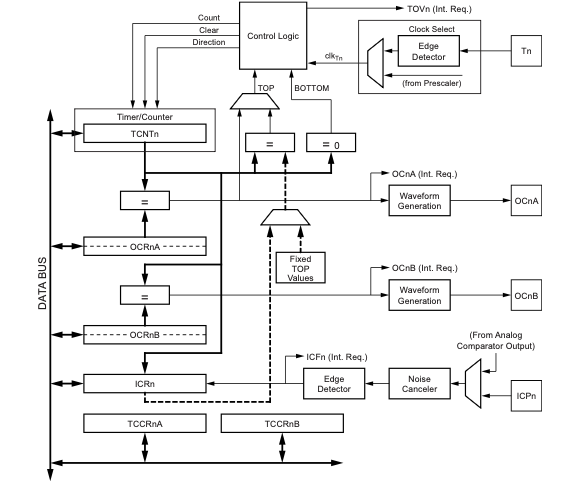
Timer 1 Block Diagram
Key components:
- Clock Select - Choose prescaler
- TCNT1 - 16-bit counter register
- OCR1A/B - Compare registers
- ICR1 - Input capture register
- Waveform Generator - Controls output pins
- Comparators - Hardware "if statements"
Key Registers for Timer 1
Data Registers
| Register | Purpose | Details |
|---|---|---|
TCNT1 |
Current count value (16-bit) | Readable/writable. Holds the live counter value (0–65535). Write to it to preset the counter; read it to snapshot the current count. |
OCR1A |
Compare value, Channel A | When TCNT1 == OCR1A, a compare-match event fires. Used as TOP in CTC & some PWM modes. Controls duty cycle on OC1A (Pin 9). |
OCR1B |
Compare value, Channel B | Independent second compare channel. Controls duty cycle on OC1B (Pin 10). Cannot define TOP. |
ICR1 |
Input Capture Register | Hardware copies TCNT1 into ICR1 on an edge at the ICP1 pin (Pin 8). Also usable as TOP in some PWM modes. |
Control & Interrupt Registers
| Register | Purpose | Details |
|---|---|---|
TCCR1A |
Control Register A | Sets compare-output mode (COM bits) and lower WGM bits. Determines what happens to OC1A/OC1B pins on a match. |
TCCR1B |
Control Register B | Sets clock source/prescaler (CS bits), upper WGM bits, and input-capture edge/noise settings. |
TIMSK1 |
Interrupt Mask | Bit-flags to enable specific interrupts: overflow (TOIE1), compare-match A/B (OCIE1A/B), input capture (ICIE1). |
TIFR1 |
Interrupt Flags | Hardware sets these when an event occurs. Cleared automatically when the ISR runs, or write a 1 to clear manually. |
// --- Quick-reference examples ---

  // Read the current timer count
  uint16_t now = TCNT1;

  // Preset the counter to a known value
  TCNT1 = 0;

  // Set a compare value (1 Hz with prescaler 1024)
  OCR1A = 15624;

  // Set a second compare for 50 % duty
  OCR1B = 7812;

  // Read the captured timestamp after
  // an external edge on ICP1 (Pin 8)
  uint16_t stamp = ICR1;

  // Configure CTC mode, prescaler 1024
  TCCR1A = 0;                        // WGM11:10 = 00
  TCCR1B = (1 << WGM12)              // CTC mode
         | (1 << CS12) | (1 << CS10);// /1024

  // Enable compare-match A interrupt
  TIMSK1 = (1 << OCIE1A);

  // Check if overflow happened (polling)
  if (TIFR1 & (1 << TOV1)) {
    TIFR1 = (1 << TOV1); // clear flag
}uint16_t now = TCNT1;— Read the timer's current count (like glancing at a stopwatch).TCNT1 = 0;— Reset the counter back to zero.OCR1A = 15624;— Tell the timer: "trigger an event when you count to 15624." With a 1024 prescaler and 16 MHz clock, this gives exactly 1 second.OCR1B = 7812;— A second, independent trigger point (halfway to 15624 = 50% duty cycle on Channel B).uint16_t stamp = ICR1;— Read the timestamp that was automatically saved when an external signal edge hit Pin 8.TCCR1A = 0;— Clear Control Register A (sets lower waveform bits to 00).TCCR1B = (1 << WGM12) | (1 << CS12) | (1 << CS10);— Two things at once: enable CTC mode (WGM12 bit) and set the prescaler to 1024 (CS12 + CS10 bits). The timer now counts in CTC mode, ticking once every 1024 CPU cycles.TIMSK1 = (1 << OCIE1A);— Enable the compare-match A interrupt. Now when TCNT1 reaches OCR1A, the CPU will automatically jump to the ISR.if (TIFR1 & (1 << TOV1))— Check if the overflow flag is set (polling instead of using an interrupt).TIFR1 = (1 << TOV1);— Clear the overflow flag by writing a 1 to it (this is how AVR flag clearing works — you write 1, not 0).
Register Walkthrough – Scenarios
Now that we know the registers, let's see how they work together in three common real-world situations. Each scenario shows a different Timer 1 capability: generating timed interrupts (CTC mode), measuring an external signal (Input Capture), and controlling two outputs at different duty cycles (Fast PWM). Pay attention to which registers are configured and why.
Scenario 1 — Periodic 10 ms Interrupt (100 Hz)
OCR1A = (16 000 000 / 64 / 100) − 1 = 2499Prescaler 64, CTC mode → compare-match every 10 ms.
Scenario 2 — Measure Pulse Width
ICR1, then switch to falling edge and read again. The difference × tick period = pulse width.
Scenario 3 — Two Independent PWM Channels
ICR1 = TOP) to set frequency, then write different duty-cycle values to OCR1A and OCR1B for pins 9 & 10 independently.
TCNT1, OCR1A/B, and ICR1 are 16-bit. The compiler handles byte ordering, but in ISRs or inline assembly you must write the high byte first and read the low byte first (the TEMP register mechanism).
// Scenario 1 – 100 Hz interrupt
  cli();
  TCCR1A = 0;
  TCCR1B = (1 << WGM12)            // CTC
         | (1 << CS11) | (1 << CS10); // /64
  OCR1A  = 2499;
  TIMSK1 = (1 << OCIE1A);
  sei();

  // Scenario 2 – Pulse width via Input Capture
  TCCR1A = 0;
  TCCR1B = (1 << ICES1)  // rising edge
         | (1 << CS11);  // /8  → 0.5 µs tick
  TIMSK1 = (1 << ICIE1); // capture interrupt

  volatile uint16_t riseTime, fallTime;
  ISR(TIMER1_CAPT_vect) {
    if (TCCR1B & (1 << ICES1)) {
      riseTime = ICR1;
      TCCR1B &= ~(1 << ICES1); // next: falling
    } else {
      fallTime = ICR1;
      TCCR1B |= (1 << ICES1);  // next: rising
    }
  }
  // pulseWidth_us = (fallTime-riseTime)*0.5;

  // Scenario 3 – Dual PWM on Pins 9 & 10
  TCCR1A = (1 << COM1A1) | (1 << COM1B1)
         | (1 << WGM11);       // Fast PWM mode 14
  TCCR1B = (1 << WGM13) | (1 << WGM12)
         | (1 << CS11);        // /8
  ICR1   = 39999;  // TOP → 50 Hz (servo)
  OCR1A  = 3000;   // Pin 9 duty
  OCR1B  = 1500;   // Pin 10 duty
Key Registers for Timer 1
| Register | Name | Purpose |
|---|---|---|
TCNT1 |
Timer/Counter 1 | Current count value (16-bit) |
OCR1A |
Output Compare Register 1A | Compare value for channel A |
OCR1B |
Output Compare Register 1B | Compare value for channel B |
ICR1 |
Input Capture Register 1 | Captures timer value on external event |
TCCR1A |
Timer/Counter Control Register A | Waveform generation, compare output modes |
TCCR1B |
Timer/Counter Control Register B | Clock select, WGM bits |
TIMSK1 |
Timer Interrupt Mask | Enable/disable interrupts |
TIFR1 |
Timer Interrupt Flag | Interrupt status flags |
TCCR1A Register
Timer/Counter1 Control Register A
| Bit 7 | Bit 6 | Bit 5 | Bit 4 | Bit 3 | Bit 2 | Bit 1 | Bit 0 |
|---|---|---|---|---|---|---|---|
| COM1A1 | COM1A0 | COM1B1 | COM1B0 | - | - | WGM11 | WGM10 |
COM1A[1:0] / COM1B[1:0] - Compare Output Mode:
| COM1x1 | COM1x0 | Description (Non-PWM) |
|---|---|---|
| 0 | 0 | Normal port operation, OC1x disconnected |
| 0 | 1 | Toggle OC1x on Compare Match |
| 1 | 0 | Clear OC1x on Compare Match (set low) |
| 1 | 1 | Set OC1x on Compare Match (set high) |
TCCR1B Register
Timer/Counter1 Control Register B
| Bit 7 | Bit 6 | Bit 5 | Bit 4 | Bit 3 | Bit 2 | Bit 1 | Bit 0 |
|---|---|---|---|---|---|---|---|
| ICNC1 | ICES1 | - | WGM13 | WGM12 | CS12 | CS11 | CS10 |
CS1[2:0] - Clock Select (Prescaler):
| CS12 | CS11 | CS10 | Description |
|---|---|---|---|
| 0 | 0 | 0 | No clock (Timer stopped) |
| 0 | 0 | 1 | clk/1 (No prescaling) |
| 0 | 1 | 0 | clk/8 |
| 0 | 1 | 1 | clk/64 |
| 1 | 0 | 0 | clk/256 |
| 1 | 0 | 1 | clk/1024 |
Waveform Generation Mode (WGM)
WGM bits are split across TCCR1A and TCCR1B:
| Mode | WGM13 | WGM12 | WGM11 | WGM10 | Mode Name | TOP |
|---|---|---|---|---|---|---|
| 0 | 0 | 0 | 0 | 0 | Normal | 0xFFFF |
| 4 | 0 | 1 | 0 | 0 | CTC (OCR1A) | OCR1A |
| 5 | 0 | 1 | 0 | 1 | Fast PWM, 8-bit | 0x00FF |
| 6 | 0 | 1 | 1 | 0 | Fast PWM, 9-bit | 0x01FF |
| 7 | 0 | 1 | 1 | 1 | Fast PWM, 10-bit | 0x03FF |
| 14 | 1 | 1 | 1 | 0 | Fast PWM (ICR1) | ICR1 |
| 15 | 1 | 1 | 1 | 1 | Fast PWM (OCR1A) | OCR1A |
Timer Interrupt Registers
TIMSK1 - Timer Interrupt Mask Register
| Bit | Name | Description |
|---|---|---|
| 5 | ICIE1 | Input Capture Interrupt Enable |
| 2 | OCIE1B | Output Compare B Match Interrupt Enable |
| 1 | OCIE1A | Output Compare A Match Interrupt Enable |
| 0 | TOIE1 | Timer Overflow Interrupt Enable |
TIFR1 - Timer Interrupt Flag Register
| Bit | Name | Description |
|---|---|---|
| 5 | ICF1 | Input Capture Flag |
| 2 | OCF1B | Output Compare B Match Flag |
| 1 | OCF1A | Output Compare A Match Flag |
| 0 | TOV1 | Timer Overflow Flag |
Setting Up Timer 1 CTC Interrupt
Here we configure Timer 1 to count up to a specific value and then automatically reset to 0, triggering an interrupt each time it matches. This creates a precise, repeating time interval — like a programmable alarm clock inside the chip.
Steps to configure a timer interrupt:
- Clear timer control registers
- Set CTC mode (WGM12 = 1)
- Set prescaler value
- Set compare match value (OCR1A)
- Enable compare match interrupt
- Enable global interrupts
|= (1 << BIT_NAME)
This pattern is how we set a single bit inside a register without changing the other bits. Let's break it down step by step:
WGM12is just a constant = 3 (it's bit number 3 in TCCR1B).(1 << WGM12)means "shift the number 1 left by 3 positions":
00000001→ shift left 3 →00001000(this creates a mask with only bit 3 set)TCCR1B |= 00001000means "OR the register with this mask":
TCCR1B:00000000
mask:00001000
result:00001000— bit 3 is now ON, all others unchanged.
Why |= and not =? Using = would overwrite all 8 bits. Using |= (OR-equals) only turns ON the bits in the mask while leaving everything else untouched.
void setup() {
  // Disable interrupts during setup
  cli();

  // Reset Timer 1 control registers
  TCCR1A = 0;
  TCCR1B = 0;
  TCNT1 = 0;  // Reset counter

  // Set compare match value for 1 Hz
  // OCR1A = (16MHz / (prescaler * freq)) - 1
  // OCR1A = (16000000 / (1024 * 1)) - 1 = 15624
  OCR1A = 15624;

  // Set CTC mode (WGM12 = 1)
  TCCR1B |= (1 << WGM12);

  // Set prescaler to 1024
  TCCR1B |= (1 << CS12) | (1 << CS10);

  // Enable compare match interrupt
  TIMSK1 |= (1 << OCIE1A);

  // Enable global interrupts
  sei();
}
Timer ISR Example
Complete example: Blink LED at 1 Hz using Timer 1
- ISR is called every 1 second
- Toggle LED state in ISR
- No code needed in loop()
ISR(TIMER1_COMPA_vect) for Timer 1 Compare Match A interrupt
#define LED_PIN 13

volatile bool ledState = false;

// Timer 1 Compare Match A ISR
ISR(TIMER1_COMPA_vect) {
  ledState = !ledState;
  digitalWrite(LED_PIN, ledState);
}

void setup() {
  pinMode(LED_PIN, OUTPUT);

  cli();  // Disable interrupts

  TCCR1A = 0;
  TCCR1B = 0;
  TCNT1 = 0;

  OCR1A = 15624;  // 1 Hz @ 1024 prescaler

  TCCR1B |= (1 << WGM12);  // CTC mode
  TCCR1B |= (1 << CS12) | (1 << CS10);  // 1024
  TIMSK1 |= (1 << OCIE1A);  // Enable int

  sei();  // Enable interrupts
}

void loop() {
  // Nothing here - timer handles everything!
}
Calculating Timer Values
Given: fCPU = 16 MHz, Desired interrupt rate
Example Calculations:
| Desired Frequency | Prescaler | OCR1A Value | Formula |
|---|---|---|---|
| 1 Hz (1 sec) | 1024 | 15624 | (16M / 1024 / 1) - 1 |
| 10 Hz (100 ms) | 1024 | 1561 | (16M / 1024 / 10) - 1 |
| 100 Hz (10 ms) | 64 | 2499 | (16M / 64 / 100) - 1 |
| 1000 Hz (1 ms) | 64 | 249 | (16M / 64 / 1000) - 1 |
Double Buffering
Compare registers (OCR1A/B) are double buffered:
- Two copies of the register exist in hardware
- You write to the "buffer" register
- Hardware uses the "active" register
- Buffer copied to active at safe time (TOP/BOTTOM)
- No glitches when updating compare values
- Atomic updates even for 16-bit values
- Safe to change values at any time
Input Capture Mode
Measure external events with hardware precision:
- External event triggers capture
- TCNT1 value copied to ICR1 instantly
- Measure pulse width, frequency, period
- Hardware timestamping - no software delay!
- Measuring signal frequency
- Pulse width measurement
- RPM sensing
- Ultrasonic distance sensors
PWM as Digital-to-Analog Converter
Convert PWM to analog voltage with an RC filter:
- PWM frequency >> RC cutoff frequency
- Capacitor smooths the pulsed signal
- Output voltage = VCC × Duty Cycle
APIs vs. Direct Register Access
| Arduino API | Direct Register Access | |
|---|---|---|
| Ease of Use | Very easy | Complex |
| Flexibility | Limited | Full control |
| Portability | Works across Arduino boards | Chip-specific |
| Performance | Overhead from abstraction | Maximum efficiency |
| Learning | Quick start | Deep understanding required |
- Need features not exposed by API
- Performance-critical applications
- Complex timing requirements
- Custom PWM frequencies/resolutions
Third-Party Timer Libraries
Simplify timer usage without full register knowledge:
- TimerOne - Easy Timer 1 interrupts
- TimerThree - For boards with Timer 3
- MsTimer2 - Millisecond-based Timer 2
- FlexiTimer2 - Flexible timing
// Using TimerOne library
#include <TimerOne.h>

void blinkLED() {
  digitalWrite(13, !digitalRead(13));
}

void setup() {
  pinMode(13, OUTPUT);

  // Initialize Timer1 to 1 second
  Timer1.initialize(1000000);  // microseconds

  // Attach interrupt function
  Timer1.attachInterrupt(blinkLED);
}

void loop() {
  // Your other code here
}
Interactive PWM Demonstration
Adjust the parameters to see how they affect the PWM signal:
Average Voltage: 2.50 V
Common Timer Mistakes
Timer Best Practices
Summary
- Timers are hardware counters that operate independently of the CPU
- ATmega328P has 3 timers: Timer 0 (8-bit), Timer 1 (16-bit), Timer 2 (8-bit)
- Prescalers divide the clock to achieve longer timing periods
- CTC mode is ideal for generating periodic interrupts
- PWM modes create analog-like signals for motor/LED control
- Key registers: TCNTn, OCRnA/B, TCCRnA/B, TIMSKn
- Be aware of resource conflicts with Arduino library functions
- Use direct register access for maximum control and flexibility
Questions?
🤔
Review the ATmega328P datasheet sections on Timer/Counter 1
Exercise: CTC Timer Setup
"Hello!" to the Serial Monitor.
The CPU clock is 16 MHz. You must:
- Choose an appropriate prescaler.
- Calculate the OCR1A value (must fit in 16 bits: 0–65535).
- Set the correct bits in TCCR1A, TCCR1B, and TIMSK1.
CTC Interrupt Frequency Formula:
Register Reference Tables
TCCR1A — Timer/Counter1 Control Register A
| Bit 7 | Bit 6 | Bit 5 | Bit 4 | Bit 3 | Bit 2 | Bit 1 | Bit 0 |
|---|---|---|---|---|---|---|---|
| COM1A1 | COM1A0 | COM1B1 | COM1B0 | — | — | WGM11 | WGM10 |
TCCR1B — Timer/Counter1 Control Register B
| Bit 7 | Bit 6 | Bit 5 | Bit 4 | Bit 3 | Bit 2 | Bit 1 | Bit 0 |
|---|---|---|---|---|---|---|---|
| ICNC1 | ICES1 | — | WGM13 | WGM12 | CS12 | CS11 | CS10 |
Waveform Generation Mode (WGM) — CTC options
| Mode | WGM13 | WGM12 | WGM11 | WGM10 | Description | TOP |
|---|---|---|---|---|---|---|
| 0 | 0 | 0 | 0 | 0 | Normal | 0xFFFF |
| 4 | 0 | 1 | 0 | 0 | CTC | OCR1A |
| 12 | 1 | 1 | 0 | 0 | CTC | ICR1 |
Clock Select (Prescaler)
| CS12 | CS11 | CS10 | Description |
|---|---|---|---|
| 0 | 0 | 0 | No clock (timer stopped) |
| 0 | 0 | 1 | clk / 1 (no prescaling) |
| 0 | 1 | 0 | clk / 8 |
| 0 | 1 | 1 | clk / 64 |
| 1 | 0 | 0 | clk / 256 |
| 1 | 0 | 1 | clk / 1024 |
TIMSK1 — Timer Interrupt Mask Register
| Bit | Name | Description |
|---|---|---|
| 5 | ICIE1 | Input Capture Interrupt Enable |
| 2 | OCIE1B | Output Compare B Match Interrupt Enable |
| 1 | OCIE1A | Output Compare A Match Interrupt Enable |
| 0 | TOIE1 | Overflow Interrupt Enable |
Exercise: Fill in the Code
Using the register tables from the previous slide, complete the code so that "Hello!" prints to Serial every 500 ms.
- Pick a prescaler so the OCR1A value fits in 16 bits.
- Calculate:
OCR1A = (16,000,000 / (prescaler × 2)) − 1 - Set WGM bits for CTC mode (mode 4).
- Set CS bits for your chosen prescaler.
- Enable the compare-match A interrupt in TIMSK1.
volatile bool printFlag = false;

ISR(TIMER1_COMPA_vect) {
  printFlag = true;
}

void setup() {
  Serial.begin(9600);
  cli();

  // 1. Reset registers
  TCCR1A = ___;
  TCCR1B = ___;
  TCNT1  = ___;

  // 2. Set compare value for 500 ms (2 Hz)
  //    OCR1A = ???
  OCR1A = ___;

  // 3. Set CTC mode
  //    Which bit(s) go in TCCR1A?  ___
  //    Which bit(s) go in TCCR1B?  ___
  TCCR1B |= (1 << ___);

  // 4. Set prescaler
  //    Which CS bits do you need?
  TCCR1B |= (1 << ___) | (1 << ___);

  // 5. Enable compare match A interrupt
  TIMSK1 |= (1 << ___);

  sei();
}

void loop() {
  if (printFlag) {
    printFlag = false;
    Serial.println("Hello!");
  }
}