Using Timer & Interrupt Arduino APIs
DE6417 Microcontrollers 2
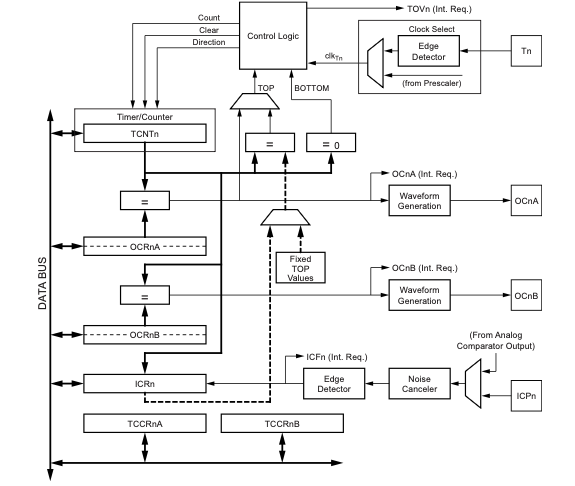
Pin Change Interrupts & Hardware Timer Control
Learning Objectives
- Review timer fundamentals and CTC (Clear Timer on Compare) mode
- Explore Arduino timer libraries and APIs
- Use the TimerOne library for simplified interrupt setup
- Drive GPIO pins directly with hardware timer outputs
- Implement real-time frequency adjustment using a potentiometer
- Understand the trade-offs between library use and direct register access
- Preview Pin Change Interrupts (PCINT)
Timer Fundamentals Review
- Timer1 is a 16-bit timer on ATmega328P
- Can generate interrupts at programmable frequencies
- Previous lecture: toggled LED in ISR, measured with oscilloscope
- Timer has multiple operating modes controlled by
TCCR1AandTCCR1Bregisters
Key Concept: Timers count clock cycles and trigger events when reaching specific values.
Timer Modes: Normal, CTC & Fast PWM
Normal Mode
- Counter counts from 0 to MAX (65535 for 16-bit)
- Interrupt triggers when counter matches OCR1A value
- Counter continues counting (doesn't reset)
CTC Mode (Clear Timer on Compare)
- Counter automatically resets to 0 when it hits OCR1A
- OCR1A becomes the "TOP" value
- No manual counter reset needed in ISR
Fast PWM Mode
- Counter counts from 0 to TOP, then resets to 0
- Output pin set at BOTTOM, cleared when counter matches OCR1A
- Produces a variable duty-cycle waveform
- Higher frequency than Phase Correct PWM
The Challenge with Raw Timer Programming
- Timer registers are complex with many configuration bits
- Reading documentation takes hours or days
- Simple tasks like "generate 1kHz interrupt" require extensive setup
- Different timers (Timer0, Timer1, Timer2) have different capabilities
Finding Arduino Libraries
- Go to Tools → Manage Libraries in Arduino IDE
- Or visit Arduino Library documentation online
- Over 200+ community-contributed libraries available
- Search for "timer" reveals many options:
- Arduino Timer Library
- Async Timer
- TimerOne (our focus)
🔧 Arduino Library Manager
Search: timer
✓ TimerOne by Paul Stoffregen
The TimerOne Library
- Created by Paul Stoffregen (Teensy developer)
- Works with ATmega168, ATmega328, and Arduino Mega
- Provides simple API for Timer1 control
Key Functions:
Timer1.initialize(microseconds)- Set the timer periodTimer1.attachInterrupt(callback)- Set ISR callbackTimer1.pwm(pin, duty)- PWM output on pin 9 or 10Timer1.detachInterrupt()- Disable interruptTimer1.disablePwm(pin)- Disable PWM
Understanding the duty parameter:
The duty value is a 10-bit number (0–1023), just like analogRead(). The library maps it so that:
0= 0% duty cycle (always LOW)512= 50% duty cycle (HIGH half the time) — because 512/1023 ≈ 50%1023= 100% duty cycle (always HIGH)
// Include the library
#include <TimerOne.h>

void setup() {
  pinMode(10, OUTPUT);

  // Initialize for 500ms period
  Timer1.initialize(500000);

  // Set 50% duty cycle on pin 9
  // duty range: 0 (off) to 1023 (full on)
  // 512 / 1023 ≈ 50%
  Timer1.pwm(9, 512);

  // Attach interrupt callback
  Timer1.attachInterrupt(myCallback);
}

void myCallback() {
  // Called every 500ms
  digitalWrite(10, !digitalRead(10));
}
TimerOne Output Signals
From the previous code example, here are the two output waveforms:
Simplified Timer Setup
With TimerOne, a 100Hz interrupt needs just 2 lines of code:
Timer1.initialize(10000)- 10,000 µs = 100 HzTimer1.attachInterrupt(callback)
Important Notes:
- The
Timer1object is pre-created by the library - Callback is a regular function, not an ISR macro
- Library handles ISR internally, calls your function
- Keep
volatilefor shared variables (good practice)
#include <TimerOne.h>

#define LED_PIN 8

volatile bool ledState = false;
volatile unsigned long interruptCounter = 0;

void blinkCallback() {
  ledState = !ledState;
  digitalWrite(LED_PIN, ledState);
  interruptCounter++;
}

void setup() {
  Serial.begin(9600);
  pinMode(LED_PIN, OUTPUT);

  // 10,000 µs = 10 ms = 100 Hz
  Timer1.initialize(10000);
  Timer1.attachInterrupt(blinkCallback);
}

void loop() {
  Serial.print("Count: ");
  Serial.println(interruptCounter);
  delay(500);
}
Understanding Interrupt vs Output Frequency
$f_{output} = \frac{f_{interrupt}}{2}$
Why divide by 2?
- Each interrupt toggles the LED (HIGH → LOW or LOW → HIGH)
- One complete cycle = 2 toggles (2 interrupts)
- Example: 100 Hz interrupt → 50 Hz LED blink frequency
| Period (µs) | Interrupt Freq | Output Freq |
|---|---|---|
| 10,000 | 100 Hz | 50 Hz |
| 5,000 | 200 Hz | 100 Hz |
| 1,000 | 1 kHz | 500 Hz |
Real-time Frequency Adjustment
Two approaches to update frequency dynamically:
Method 1: Update in ISR
- Read potentiometer in
loop() - Update OCR1A in ISR for immediate effect
Method 2: Update in Main Loop
- Works even without ISR (pure hardware mode)
- Direct write to OCR1A register
- Change takes effect on next compare match
WGM12 = 1 in TCCR1B. OC1A pin toggles on match via COM1A0 = 1 in TCCR1A.
// Method 2: Pure hardware + main loop update
#define POT_PIN A5

void setup() {
  // Set PB1 (Arduino Pin 9) as OUTPUT
  // DDRB = Data Direction Register for Port B
  // PB1 = bit 1 of Port B = Arduino digital pin 9
  // This pin is also the OC1A hardware output
  DDRB |= (1 << PB1);
  // Arduino equivalent: pinMode(9, OUTPUT);

  // Toggle OC1A on compare match
  TCCR1A = (1 << COM1A0);

  // CTC mode (WGM12) + no prescaler (CS10)
  TCCR1B = (1 << WGM12) | (1 << CS10);

  OCR1A = 8000;  // Initial compare value
}

void loop() {
  uint16_t adc = analogRead(POT_PIN);

  // Map 0-1023 to 1000-32000
  uint16_t newOCR = map(adc, 0, 1023,
                         1000, 32000);

  // Atomic update (16-bit register)
  noInterrupts();
  OCR1A = newOCR;
  interrupts();

  delay(10);  // Debounce
}
Achievable Frequency Range
With potentiometer mapped to OCR1A values 1000-32000:
| OCR1A Value | Interrupt Freq | Toggle Output |
|---|---|---|
| 32,000 | 500 Hz | 250 Hz |
| 16,000 | 1 kHz | 500 Hz |
| 8,000 | 2 kHz | 1 kHz |
| 1,000 | 16 kHz | 8 kHz |
Formula: f = 16,000,000 / (2 × OCR1A)
The Big Idea: PWM → Any Waveform
A digital pin can only be HIGH (5V) or LOW (0V). But by changing the duty cycle over time, we control the average voltage at each instant.
📊
Duty Cycle = Amplitude
$V_{avg} = V_{cc} \times D$
⏱️
Update Rate = Resolution
Timer ISR updates duty at fixed intervals
🔄
Pattern = Waveform
How duty changes over time defines the shape
Square Wave via PWM
The simplest waveform — duty cycle alternates between 0% and 100%:
#define PWM_PIN 9   // OC1A output pin
#define POT_PIN A0  // Potentiometer input

// 'volatile' because these are shared
// between ISR and main loop
volatile uint16_t halfPeriod = 20;
volatile uint16_t counter = 0;
volatile bool high = false;

// Runs every 25µs (40 kHz)
ISR(TIMER1_COMPA_vect) {
  counter++;  // Count ISR calls
  // When we've counted enough calls,
  // toggle the output state
  if (counter >= halfPeriod) {
    high = !high;   // Flip HIGH↔LOW
    counter = 0;    // Reset counter
  }
  // Set duty to 100% or 0% based on state
  if (high) {
    analogWrite(PWM_PIN, 255);  // 100% duty
  } else {
    analogWrite(PWM_PIN, 0);    // 0% duty
  }
}

void setup() {
  pinMode(PWM_PIN, OUTPUT);

  TCCR1A = 0;  // Clear control register A
  // CTC mode (auto-reset at OCR1A)
  // No prescaler (16 MHz clock)
  TCCR1B = (1 << WGM12) | (1 << CS10);
  // 16MHz / (399+1) = 40 kHz ISR rate
  OCR1A = 399;
  // Enable compare match interrupt
  TIMSK1 = (1 << OCIE1A);
}

void loop() {
  // Read pot (0–1023)
  uint16_t adc = analogRead(POT_PIN);
  // Protect 16-bit write from ISR
  noInterrupts();
  // Map pot to square wave speed
  // Low value = fast, high = slow
  halfPeriod = map(adc, 0, 1023, 5, 200);
  interrupts();
}
Triangle Wave via PWM
Duty cycle ramps up from 0→255, then ramps down 255→0 linearly:
// Triangle wave generation
// duty ramps: 0→255→0→255→...
static uint8_t duty = 0;
static int8_t direction = 1; // +1=up, -1=down

// stepSize controls the waveform frequency
// Read from pot in loop() (not shown)
ISR(TIMER1_COMPA_vect) {
  // Increase or decrease duty each tick
  duty += direction * stepSize;

  // Hit the top → reverse to ramp down
  if (duty >= 255) {
    duty = 255;
    direction = -1;
  }
  // Hit the bottom → reverse to ramp up
  else if (duty <= 0) {
    duty = 0;
    direction = 1;
  }

  // Set PWM duty cycle on Pin 9
  // duty=0 → 0V avg, duty=255 → 5V avg
  analogWrite(9, duty);
}

// stepSize=1 → 512 ISR calls per cycle
// stepSize=4 → 128 ISR calls per cycle
// Higher stepSize = higher frequency
Sine Wave via PWM (SPWM)
Use a Look-Up Table of pre-calculated sine values to set the duty cycle:
// Look-Up Table: one full sine cycle
// 64 samples, values 0–255 (8-bit PWM)
// Formula: LUT[i] = 127 + 127×sin(2π×i/64)
// Stored in flash (const) to save RAM
const uint8_t sineTable[64] = {
  128,140,153,165,176,187,197,205,
  213,219,224,228,231,233,234,234,
  233,231,228,224,219,213,205,197,
  187,176,165,153,140,128,115,102,
   90, 79, 68, 58, 50, 42, 36, 31,
   27, 24, 22, 21, 21, 22, 24, 27,
   31, 36, 42, 50, 58, 68, 79, 90,
  102,115 };

static uint16_t index = 0;
// 'speed' set from pot in loop()

ISR(TIMER1_COMPA_vect) {
  // Read next duty value from table
  analogWrite(9, sineTable[index]);
  // Advance index by 'speed' steps
  // Wraps around using modulo (%)
  index = (index + speed) % 64;
}

// speed=1 → walk through every sample
//   → slowest sine frequency
// speed=4 → skip 3 samples each time
//   → 4× faster sine frequency
🔧 Interactive: PWM Waveform Builder
Lab 1: System Architecture
Your digital signal generator uses two independent timers working together:
analogWrite) controls the PWM carrier signal. They are independent — Timer1 "shapes" the waveform by changing duty, Timer2 generates the actual PWM switching.
The Sampling Clock: Timer1 CTC Formula
The ISR must run fast enough to produce smooth waveforms. We use CTC mode (Clear Timer on Compare):
Output Compare Register value:
Rearranged for ISR frequency:
Example Calculation
Want \( f_{ISR} = 40{,}000 \) Hz
\( f_{CPU} = 16{,}000{,}000 \) Hz
Prescaler = 1 (no division)
\( \text{OCR1A} = \frac{16{,}000{,}000}{1 \times 40{,}000} - 1 = 399 \)
Why 40 kHz?
For a 50 Hz waveform with 256 steps:
Minimum ISR rate = \( 50 \times 256 = 12{,}800 \) Hz
40 kHz gives ~3× headroom, ensuring smooth output even at maximum waveform frequency.
Register Setup
TCCR1A = 0;
TCCR1B = 0;
TCNT1  = 0;
OCR1A  = 399;
TCCR1B |= (1 << WGM12);
TCCR1B |= (1 << CS10);
TIMSK1 |= (1 << OCIE1A);
PWM Average Voltage Formula
PWM is a digital signal, but its average voltage acts like an analog output:
where \( D \) = duty cycle (0 to 1), \( V_{CC} = 5\text{V} \), \( T_{on} \) = HIGH time per period
analogWrite |
Duty Cycle | \( V_{avg} \) |
|---|---|---|
| 0 | 0% | 0.00 V |
| 64 | 25% | 1.25 V |
| 127 | ~50% | 2.49 V |
| 191 | ~75% | 3.75 V |
| 255 | 100% | 5.00 V |
\(\displaystyle V_{avg} = 5 \times \frac{\text{value}}{255}\)
Controlling Waveform Frequency
The ISR rate is fixed (40 kHz). Waveform frequency is controlled by how fast we step through duty values:
Triangle wave frequency (one full cycle = 0→255→0 = 510 steps):
Sine wave frequency (LUT of N entries):
Example: Triangle at 10 Hz
Want \( f_{wave} = 10 \) Hz
\( f_{ISR} = 40{,}000 \) Hz
\( \text{stepSize} = \frac{10 \times 512}{40{,}000} = 0.128 \)
Since stepSize must be an integer ≥ 1,
min frequency ≈ \( \frac{40{,}000}{512} \approx 78 \) Hz
Solution: Use a fractional accumulator or reduce ISR rate for low frequencies.
Potentiometer Mapping
ADC reads 0–1023 from the pot.
Map to stepSize:
void loop() {
  int pot = analogRead(A0);
  // Map pot → stepSize (1–50)
  stepSize = map(pot, 0, 1023,
                 1, 50);
}
Higher stepSize → faster stepping → higher \( f_{wave} \)
Frequency Summary Table
| Step | Triangle | Sine (64) |
|---|---|---|
| 1 | 78 Hz | 625 Hz |
| 2 | 156 Hz | 1250 Hz |
| 5 | 391 Hz | 3125 Hz |
| 10 | 781 Hz | 6250 Hz |
Sine LUT with 64 entries cycles faster (fewer steps per period) than triangle with 512.
Sine Look-Up Table (LUT)
A sine wave requires non-linear duty values. Pre-compute them into a flash-stored array:
LUT entry formula (N = table size, 8-bit PWM):
Output range: 0–254 → maps to 0–100% duty → 0–5V average
Balance between smoothness and memory. 64 bytes is tiny for flash but gives \( 360° / 64 = 5.6° \) resolution — plenty smooth for audio-range signals.
const?Stores the table in flash (program memory) instead of RAM. On ATmega328P: 32 KB flash vs only 2 KB RAM.
// Pre-calculated sine look-up table
// 64 samples, stored in flash memory
// LUT[i] = 127 + 127 × sin(2π×i/64)

const uint8_t sineTable[64] = {
  128, 140, 153, 165, 176, 187, 197, 205,
  213, 219, 224, 228, 231, 233, 234, 234,
  233, 231, 228, 224, 219, 213, 205, 197,
  187, 176, 165, 153, 140, 128, 115, 102,
   90,  79,  68,  58,  50,  42,  36,  31,
   27,  24,  22,  21,  21,  22,  24,  27,
   31,  36,  42,  50,  58,  68,  79,  90,
  102, 115, 128
};

// ISR walks through the table
// 'volatile' — shared between ISR & loop
volatile uint8_t stepSize = 1;
static uint8_t idx = 0;

ISR(TIMER1_COMPA_vect) {
  // Advance index by stepSize
  // wrapping around with modulo
  idx = (idx + stepSize) % 64;

  // Set PWM duty from the table
  analogWrite(9, sineTable[idx]);
}

// In loop(): pot controls stepSize
void loop() {
  int pot = analogRead(A0);
  stepSize = map(pot, 0, 1023, 1, 20);
}
Carrier vs. Waveform Frequency
The signal generator has three frequency layers — understanding their relationship is the key insight:
1. CPU Clock
Base oscillator. Drives everything.
2. ISR Rate (Timer1)
How often duty is updated.
3. PWM Carrier (Timer2)
Hardware switching frequency.
See Your Signal: RC Low-Pass Filter
The PWM output on Pin 9 is a digital signal. To see the smooth analog waveform, add a simple RC low-pass filter:
Cut-off frequency:
Time constant:
How It Works
The capacitor charges when PWM is HIGH and discharges when LOW. If the RC time constant is much longer than the PWM period, the capacitor voltage smooths out to the average — your waveform!
Choosing R and C
Rule: \( f_c \) must be above the waveform frequency but below the PWM carrier:
\( f_{wave} \ll f_c \ll f_{PWM} \)
\( 50\text{ Hz} \ll f_c \ll 490\text{ Hz} \)
Example: R = 1 kΩ, C = 1 μF
\( f_c = \frac{1}{2\pi \times 1000 \times 0.000001} \)
\( f_c = \frac{1}{0.00628} \approx \mathbf{159\text{ Hz}} \)
✅ Well above 50 Hz (passes waveform)
✅ Well below 490 Hz (blocks carrier)
Other Combinations
| R | C | \( f_c \) |
|---|---|---|
| 1 kΩ | 1 μF | 159 Hz |
| 1 kΩ | 4.7 μF | 34 Hz |
| 10 kΩ | 100 nF | 159 Hz |
| 4.7 kΩ | 470 nF | 72 Hz |
Lower \( f_c \) = smoother output but more waveform attenuation.
Summary & Questions
We covered:
- ✅ Timer fundamentals: Normal, CTC & Fast PWM modes
- ✅ The TimerOne library — simplified timer API
- ✅ CTC mode register config & frequency formula: \( \text{OCR1A} = \frac{f_{CPU}}{\text{Prescaler} \times f_{ISR}} - 1 \)
- ✅ Real-time frequency adjustment with potentiometer
- ✅ PWM waveform shaping: square, triangle & sine (SPWM)
- ✅ Average voltage: \( V_{avg} = V_{CC} \times D \) | Sine LUT: \( \text{LUT}[i] = 127 + 127\sin(2\pi i/N) \)
- ✅ Carrier vs. waveform frequency — three frequency layers
- ✅ RC low-pass filter: \( f_c = \frac{1}{2\pi RC} \) to view your analog signal
Next: Pin Change Interrupts (PCINT)
❓ Questions?